Semiconductor Device Simulation:
With Silvacos VIRTUAL WAFER FAB we’re able to simulate:
- MOSFET-
- MESFET-
- HBT-
- HEMT-
devices with advanced materials (SiGe, GaAs, GaN or other ternary and quaternary materials). A direct impact of layer-, recess- or other modifications to the device behavior thus can easily be made visible.
Simulation Input:
Detailled device structure including (recess) dimensions, layer structure and doping profile.
Simulation Output:
– Input/output characteristics
– contour plots, e.g.
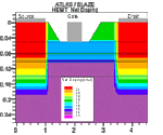
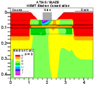
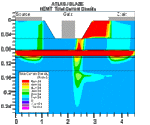
or e-field, hole concentration, potential from various working points.
Further analysis:
- Cutlines (e.g. band parameters).
- DC-analysis (e.g. threshold voltage, transconductance, subthreshold voltage).
- AC-analysis (e.g. ft, fmax, S-parameters).
- Transient analysis
Available models:
A wide range of numerous models for all these materials are (among others) available, e.g.:
- Fermi-Dirac and Boltzmann statistics
- Drift-diffusion transport models
- Energy balance transport models (velocity overshoot is included)
- Field- and doping dependend mobility
- Graded and abrupt heterojunctions
- Bandgap Narrowing and high doping effects
- Shockley-Read-Hall, Auger-and surface recombination
- Hot carrier effects
For more detailled information about SiGe hetero-FET device simulation see our Solid State Technology-publication “New approaches to a simulation-assisted design and process development” (Vol. 40, Issue 3)

